EV Group
850 SOI Wafer
The EVG 850 SOI Wafer is a fully automatic wafer bonder. The EVG 850 SOI Wafer is suitable for wafer sizes up to 6 inch/150mm. The EVG 850 SOI Wafer includes one bonding station with high vacuum.[1][2][3]

Wafer size
150mm
Vacuum
One bonding station with high vacuum[1]
What it is
The EV Group 850 SOI Wafer is a fully automatic wafer bonder in the packaging and bonding category. The machine is suitable for wafer sizes up to six inch or 150 mm and is currently configured for six inch or 150 mm wafers.[1][2][3]
The EV Group 850 SOI Wafer includes one bonding station with high vacuum, one Genmark robot with pre-aligner, and two cleaning modules. The machine uses PC control with a Windows based graphical user interface and password protected access levels.[1][2][3]
How it works
A wafer bonding system in this class typically combines wafer handling, cleaning, alignment, and a final bonding station. Cleaning modules support surface preparation, and rotational control during substrate cleaning supports the cleaning step.[1][2][3]
The EV Group 850 SOI Wafer has a mechanical pre-aligner on the bond station that is pneumatically actuated. The machine also offers a megasonic cleaning option and programmable rotational speed for substrate cleaning.[1][2][3]
Where it fits in the process flow
Applications
What do the numbers mean?
Vacuum & pumping2
- One bonding station with high vacuum[1]
Wafer handling10
Control & software3
- PC controlled with windows based graphical user interface[1]
Configuration & options12
What does it need to run?
Site utility requirements, footprint, and infrastructure needed to install and operate this tool. Sourced from public records.
Where are the manuals?
Generated from public-source data on file. Enter your email to access — nothing is published; details are routed privately.
Not publicly documented
Field notes
No research found yet — worked with this tool? Share what you know.
Frequently asked questions
What wafer size does the EV Group 850 SOI Wafer support?
The EV Group 850 SOI Wafer is suitable for wafer sizes up to six inch or 150 mm, and it is currently configured for six inch or 150 mm wafers.[1][2][3]
Is the EV Group 850 SOI Wafer fully automatic?
What handling and alignment hardware does the EV Group 850 SOI Wafer include?
The EV Group 850 SOI Wafer includes one Genmark robot with pre-aligner and a mechanical pre-aligner on the bond station that is pneumatically actuated.[1][2][3]
Not publicly documented
The following facts about the 850 SOI Wafer are absent from this record as of this revision. First-hand knowledge or a citation closes a gap; every submission is reviewed before publication.
No publicly documented production dates or lifecycle milestones (introduction, end of production, EOL) for the 850 SOI Wafer are on record.
Answerable by: OEM historical records or a trade-press announcement
No publicly documented variants, configuration options, or revision breakpoints of the 850 SOI Wafer are on record.
Answerable by: an OEM product catalog or an engineer who ordered or specified the tool
The control-system platform and OS era of the 850 SOI Wafer are not on record.
Answerable by: an engineer who operated it or OEM installation records
No publicly documented failure modes or field errata for the 850 SOI Wafer are on record.
Answerable by: a field service engineer, process engineer, or maintenance technician
The process node or technology generation of the 850 SOI Wafer is not on record.
Answerable by: an OEM datasheet or a fab qualification report
No research found yet — worked with this tool? Share what you know.
Sources & citations
Sources (3)Every fact above is drawn from these public sources
- [1]Inventory photo
- [2]waferpedia.com — waferpedia.comwaferpedia.com
- [3]lithosupport.com — lithosupport.comlithosupport.com
Last updated Oct 9, 2026.
Compare with similar tools
View all →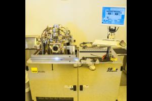
The SUSS MicroTec SB8e is a VAC substrate bonder for MEMS bonding processes.

Applied Materials model 0010-47763 is an ASSY ESC Bonded Monopolar Dual Heated unit.
The Applied Materials 0041-26723 is a bonded assembly used in semiconductor packaging and bonding applications.
The Logitech 1 WBS 1 is a wafer substrate bonder for 6-inch wafers.
