CEE
100CB
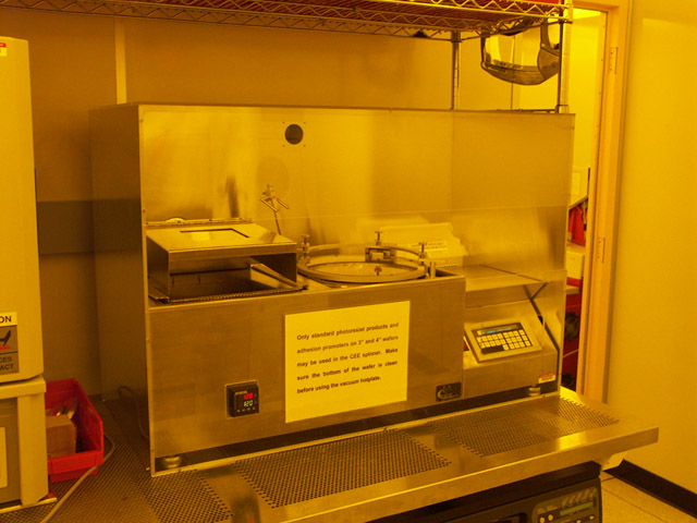
Plate 01CEE 100CB Spin Coater
Bid ServicellcWatch on YouTubePlate 02CEE Brewer Science 100CB Spin Coater Hot Plate #63142
Bid ServicellcWatch on YouTubePlate 03Cee 100CB Spin Coater & Hot Plate #61475
Bid ServicellcWatch on YouTubePlate 04Cee 100CB Spin Coater Hot Plate #62773
Bid ServicellcWatch on YouTube
Wafer size
4"
Vacuum
Mounted in an exhausted custom hood[1]
Gas delivery
Standard positive photoresists only[1]
What it is
The CEE 100CB handles substrates from 1 cm² to 4-inch wafers. The tool is intended for use with standard positive photoresists only.[1][2]
Two mounting configurations are available for the CEE 100CB. The table top version is mounted in an exhausted custom hood. The bench mounted version is mounted in an exhausted wet bench.[1][2]
How it works
The CEE 100CB is programmable with up to 10 process steps. The tool has a spin speed up to 5000 rpm. The hotplate is a programmable vacuum hotplate for baking photoresist.[1][2]
Where it fits in the process flow
General reference — not yet source-verifiedThe CEE 100CB is positioned in the photolithography process flow for applying and pre-baking photoresist before exposure. After spin coating, the substrate is typically baked on the hotplate to remove solvents. The tool can also be used for post-exposure baking.
What can it run?
Process applications and technology nodes documented for this tool.
- Photoresist baking
- Spinning substrates
What do the numbers mean?
Vacuum & pumping6
- Mounting variants
- Table top (exhausted custom hood) and Bench mount (exhausted wet bench)[1]
Wafer handling2
Gas & chemistry2
Configuration & options9
Vintage & configurations
Documented models & variants
| Designation | Generation | Vintage | Changes | Source |
|---|---|---|---|---|
| CEE 100CB Table Top Spinner/Hotplate | — | — | Table-top configuration; mounted in an exhausted custom hood. | nanofab.ece.cmu.edu[1] |
| CEE 100CB Bench Mounted Spinner/Hotplate | — | — | Bench-mounted configuration; mounted in an exhausted wet bench. | nanofab.ece.cmu.edu[2] |
| CEE 100CB Bench Mount Spinner/Hotplate | — | — | Mounted in an exhausted wet bench | nanofab.ece.cmu.edu[2] |
| CEE 100CB Table Top | — | — | Mounted in an exhausted custom hood | nanofab.ece.cmu.edu[1] |
| CEE 100CB Bench Mount | — | — | Mounted in an exhausted wet bench | nanofab.ece.cmu.edu[2] |
What does it need to run?
Site utility requirements, footprint, and infrastructure needed to install and operate this tool. Sourced from public records.
- Photoresist compatibilityStandard positive photoresists only[1]
- HotplateProgrammable vacuum hotplate for baking photoresist[1]
- MountingMounted in an exhausted custom hood[1]
- MountingMounted in an exhausted wet bench[2]
- Photoresist typeStandard positive photoresists only[1]
- Hotplate typeProgrammable vacuum hotplate for baking photoresist[1]
- Mounting variantsTable top (exhausted custom hood) or bench mount (exhausted wet bench)[2]
- Mounting variantsTable top (exhausted custom hood) and Bench mount (exhausted wet bench)[1]
Where are the manuals?
Generated from public-source data on file. Enter your email to access — nothing is published; details are routed privately.
Not publicly documented
Field notes
No research found yet — worked with this tool? Share what you know.
Frequently asked questions
What substrate sizes does the CEE 100CB handle?
The CEE 100CB handles substrates from one square centimeter to four-inch wafers.[1][2]
What photoresists is the CEE 100CB intended for?
The CEE 100CB is to be used for standard positive photoresists only.[1][2]
Not publicly documented
The following facts about the 100CB are absent from this record as of this revision. First-hand knowledge or a citation closes a gap; every submission is reviewed before publication.
No publicly documented production dates or lifecycle milestones (introduction, end of production, EOL) for the 100CB are on record.
Answerable by: OEM historical records or a trade-press announcement
The control-system platform and OS era of the 100CB are not on record.
Answerable by: an engineer who operated it or OEM installation records
No publicly documented failure modes or field errata for the 100CB are on record.
Answerable by: a field service engineer, process engineer, or maintenance technician
The process node or technology generation of the 100CB is not on record.
Answerable by: an OEM datasheet or a fab qualification report
No publicly documented compatible parts, consumables, or accessories for the 100CB are on record.
Answerable by: an OEM parts catalog or a service engineer
No research found yet — worked with this tool? Share what you know.
Sources & citations
Sources (3)Every fact above is drawn from these public sources
- [1]nanofab.ece.cmu.edu — nanofab.ece.cmu.edunanofab.ece.cmu.edu
- [2]nanofab.ece.cmu.edu — nanofab.ece.cmu.edunanofab.ece.cmu.edu
- [3]nanofab.ece.cmu.edu — nanofab.ece.cmu.edunanofab.ece.cmu.edu
Last updated Oct 3, 2026.